Right angle mounting of fuses: A small adaptor board.
So an ongoing project of mine is an autopilot for my boat. Here’s the latest incarnation:
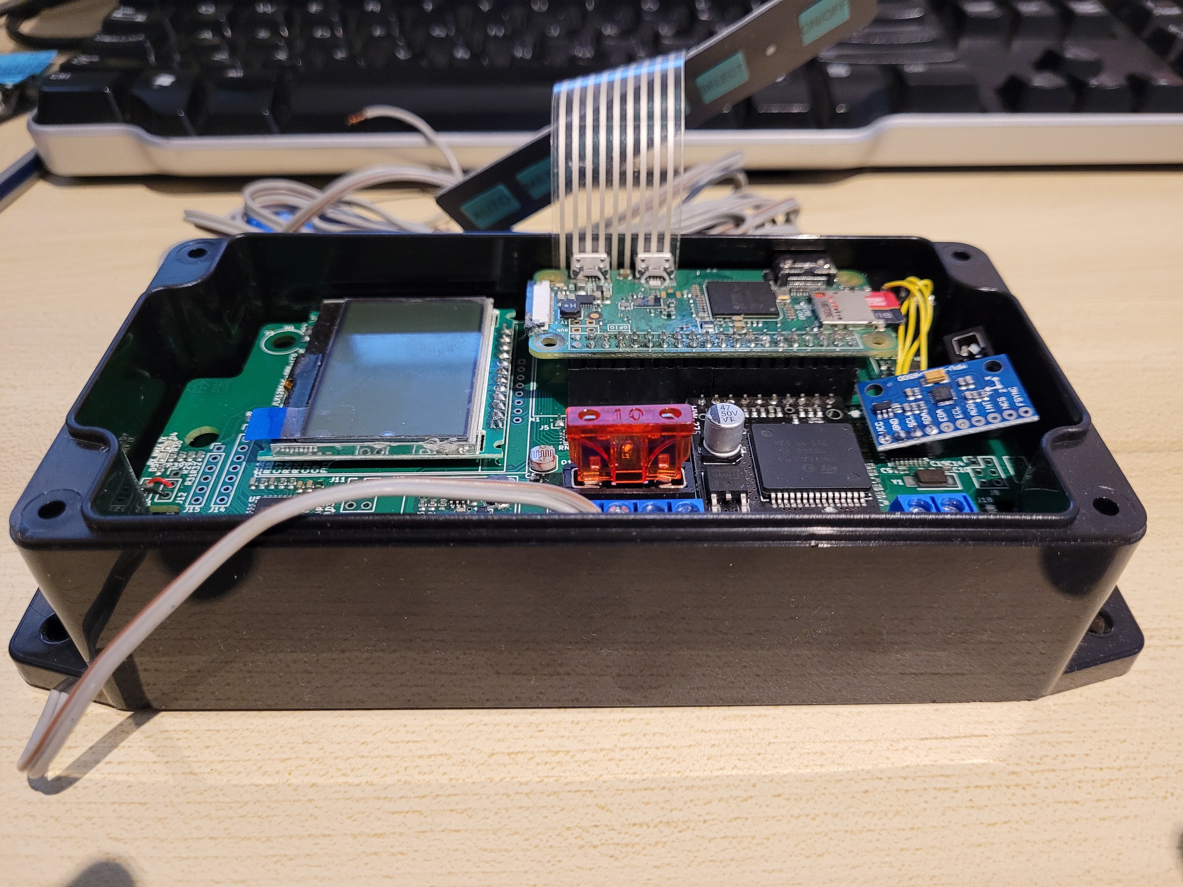
The highest point on the board is the red fuse in the middle of the board, which is made even higher by the fuse holder underneath it.
| Part | Height |
|---|---|
| Automotive fuse | 13.5mm |
| Fuse holder | 7.5mm |
| Total | 21mm |
21mm is a lot, and it’s going to interfere with the slimmer custom case I’m planning. So what can I do? Well, I’m planning to make a small PCB to mount fuses parallel to the PCB, rather than at right angles. (Actually, two PCBs because I’d like to support both standard and mini automotive fuses). By mounting the fuse on its side, I hope to get the height from 21mm down to the width of the fuse holder (7mm).
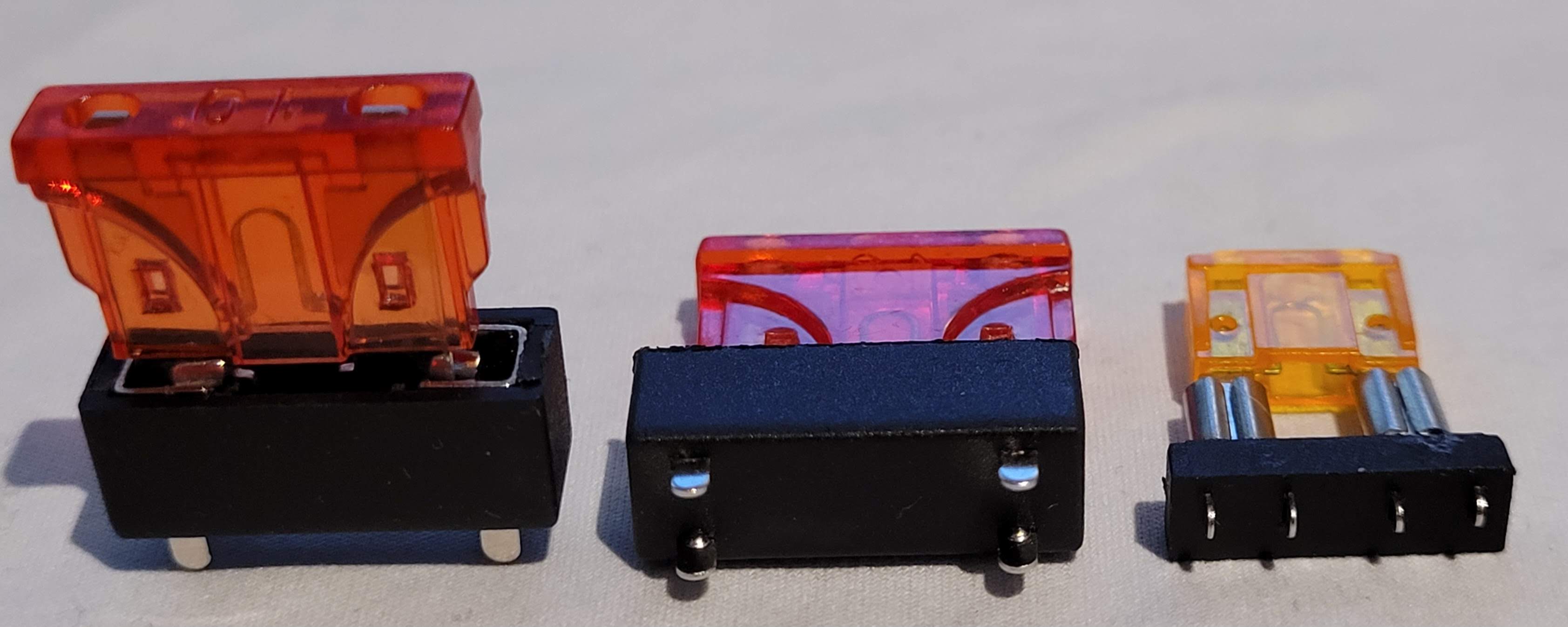
Each of the two small PCBs will have slots for a standard or mini automotive fuse, and two tinned-pad legs off to the side like an overgrown edge connector. These two legs will go down through two slots in the next revision of my autopilot. Solder will hold the legs into the slots.
As usual, I designed these boards in KiCad.
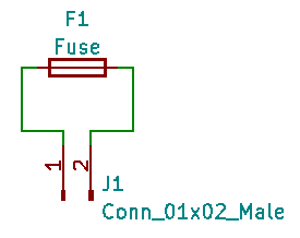
Step 1: Schematic
The schematic, which looks the same for both boards, has just the fuse (well really the fuse holder) and the legs.
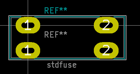
Step 2: Footprint for the standard fuse holder
Here’s the footprint for the standard fuse holder. I’ve tried this footprint out before, so I know it’s the right size. I’ve made the pads for the slots a little larger than the outline of the fuseholder, so KiCad was complaining that the teal-coloured silkscreen was being obscured by the pad. To work around this, I’ve removed the silkscreen next to the pads.
Note that for these fuse holders, the two left pads are electrically connected, and the two right pads are connected. The way to tell this to KiCad is to give the left two and the right two the same pad numbers.
Step 3: Footprint for the mini fuse holder
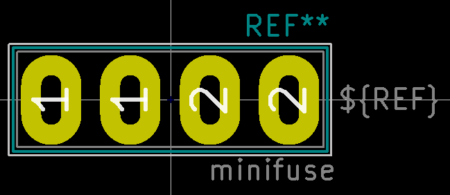
I followed a similar process to make this footprint: Take a fuse holder, measure the case and pin dimensions with digital calipers, then size the footprint dimensions accordingly.
Because this is only really possible if you have the actual part, it’s important to buy these parts ahead of time. To go from having the idea of using a part, to having a PCB which you know works with that part can mean:
- Source and buy part from China
- Wait for part to arrive
- Design footprint and/or PCB to suit actual part
- Order PCB from China
- Wait for PCBs to arrive
- (And it’s possible you’ll need to repeat this if the part isn’t suitable, or the PCB design isn’t right)
I guessed I’d want to try mini fuses, so I ordered these parts weeks ago. This process is a pipeline, and you have to keep your pipeline full!
This footprint has three rectangles. The inner grey rectangle is for the size of the part. The teal rectangle is for the silkscreen which is printed around the part. You still want to see the silkscreen when the part is in place, so it has to be a little larger. The outer light grey rectangle is the “courtyard”. It’s designed to ensure that there’s enough space between adjacent components. When doing a DRC (Design Rule Check), KiCad will complain if there are overlapping courtyards.
Step 4: Footprint for the legs which go through the main PCB
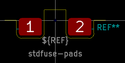
Something in common for these two boards are the legs, so I’ve put the legs, and the associated board outline near the legs, into a footprint.
Four things to note:
- I’ve chosen to interpret the horizontal origin of the footprint as where it will sit when inserted into the main PCB.
- The two little teal-coloured marks next to the pad numbers represent the edge of the main board. Above the mark will be buried in the main board slot, and below will poke out. From this I can estimate what the shape of the solder fillet will be.
- The yellow line represents the edge of the PCB. Regarding the final PCB, KiCad is happy if some of the PCB outline comes from a footprint, and some is drawn as part of the PCB. Being able to include some of the PCB outline in the footprint is super useful when the footprint is for legs like these, or you’re showing how a connector is positioned on the edge of the board.
- The board edge is lifted clear in the middle of the footprint. The gap will allow the fuse to be locked to the PCB with a small cable tie. This is to ensure the fuse can’t fall out over time with vibration or from being dropped. Without this, the autopilot could fail with no-one at the helm!
Step 5: Do layout for PCB which holds standard fuse holder
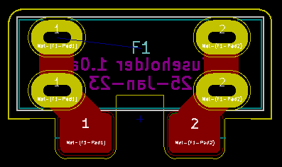
Here I’m combining the fuseholder footprint with the legs footprint. The two footprints are joined with 3mm-wide copper on this side (red colour), and 3mm copper on the other side (green, not shown). Also shown here is the rest of the board outline (the part not supplied by the legs footprint) and silkscreen showing version and date.
Step 6: Do layout for PCB which holds mini fuse holder
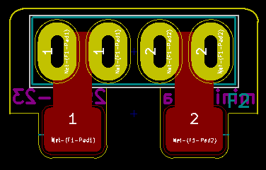
Same for the mini fuse holder. Note the arc at top right: KiCad has some harmless minor bugs regarding drawing arcs at low resolution. I suspect it’s some kind of off-by-one bug in the rendering code.
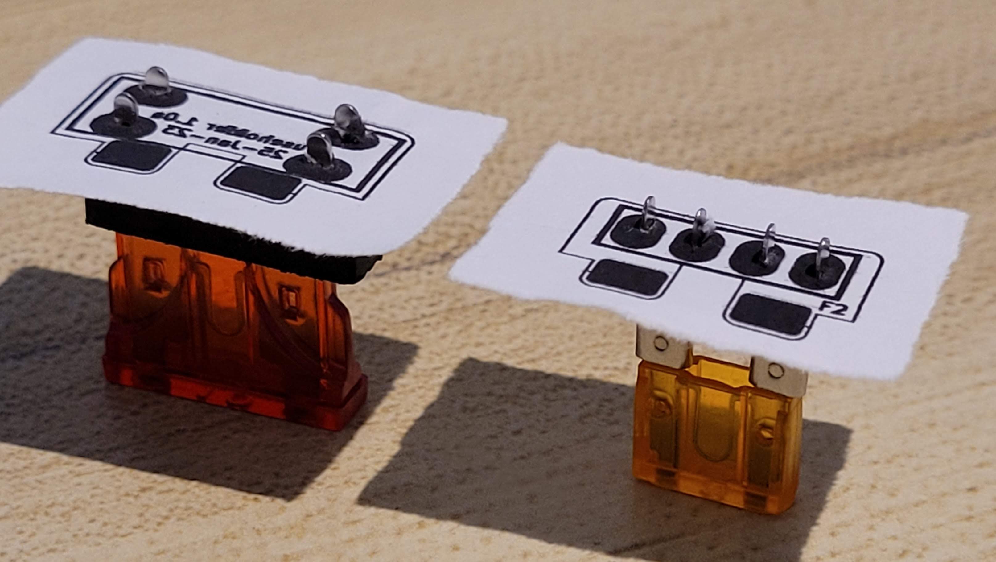
Step 7: Print on paper and do fit tests with real components
This, believe it or not, is the most important part of the whole process. The idea is to print out the PCBs on paper at 1:1 size, and make sure the components fit. Ignore this step at your own peril! What I’m looking for is that I have the component sizes right, and the sizes of the holes and/or slots are right.
Step 8: Send gerbers to JLC for manufacture
After the fit test, I use KiCad to generate gerber and drill files, then put
them into a zip file (for example, kicad-fuse-std-1.0a.zip and
kicad-fuse-mini-1.0a.zip. After uploading the zip file to JLC, the JLC
website shows a rendering of the board. Getting five of these boards is
only USD2, what a bargain.
This pic shows the two designs:
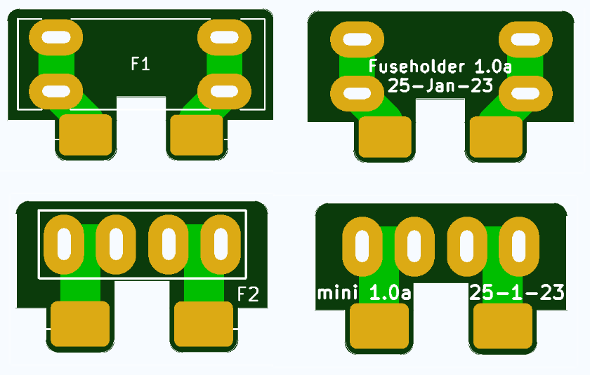
It’s interesting to note that JLC’s rendering software also has problems with the arcs in the corners of the boards, but it shouldn’t affect the final result.
Step 9: Wait for boards to arrive, measure dimensions and create footprint for main board
When these adaptor boards arrive, I’ll measure the thickness of the boards, plus the widths of the legs, and design a new footprint to go on the autopilot board. I’m looking for a nice snug fit, so I need to measure the dimensions of the actual adaptor PCBs.